Reliable and cost-effective
By applying the GaAs technology, comparable results to SiC and GaN:Si can be achieved, though at significantly lower component costs.
Thanks to the unique and comprehensively patented GaAs technology for high voltages between 600V up to 1,700V and currents up to 100A per chip, PiN- Schottky diodes, bipolar transistors as well as IGBTs can be manufactured at remarkably higher frequences than Si components.
As the first enterprise, 3-5PE has developed an industrial manufacturing process of power semiconductors for high voltages and currents that allows Gallium arsenide (GaAs) layers on GaAs substrates. This new method allows the fabrication of high- quality power semiconductors at manufacturing costs that are significantly lower than those of silicon carbide based devices.
GaAs power semiconductors can perform switching operations and energy transmissions with high voltages and high current carrying capacity much more efficiently and at higher reliability than silicon-based systems.
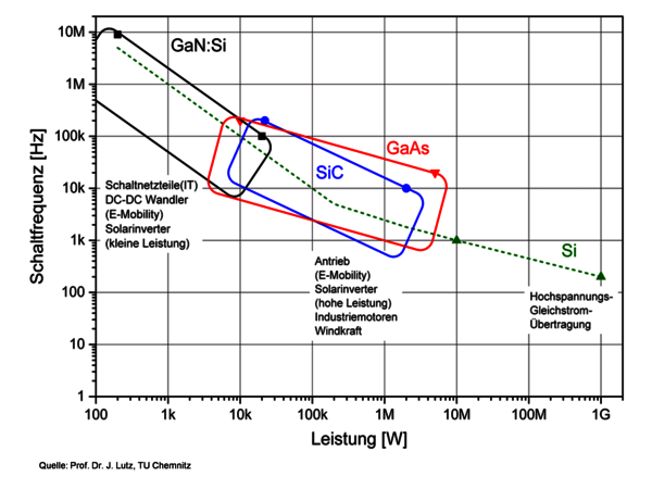
3-5PE‘s GaAs technology that has so far not been deployed in power electronics can - according to Prof. Dr. Josef Lutz, Professorship at the Faculty of Power Electronics and Electromagnetic Compatibility/ Technical University of Chemnitz - compared to materials Si, SiC and GaN/Si and classified in terms of dependence of power and switching frequency as follows:
One of the most significantly positive properties of gallium arsenide-based power semiconductors is their high carrier mobility, which is 6-7 times better than silicon and 10 times better than silicon carbide. A comparison of further parameters of gallium arsenide PiN diodes and silicon carbide Schottky diodes on the one hand, compared to silicon diodes on the other hand results in the following evaluation:
| Si | SiC | dWBG | Evaluation | |
|---|---|---|---|---|
| Breakdown voltage | O | ++ | + | 2 times better than Si |
| Electron mobility | + | O | ++ | 6 times better than Si |
| Thermal resistance | + | + | + | Up to 300°C |
| Switching losses | O | ++ | ++ | 1/7 von Si |
| Switching frequency | O | + | + | 7 times faster than Si |
| Generation of EMC disturbances | ++ | O | ++ | Comparable to Si |
Note: O indicates "more up-to-date", + = better than and ++ = significantly better than the respective parameter standard
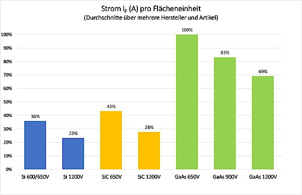
Further positive features of the GaAs diode are the forward voltage Vf, which is up to 0.5V lower compared to the typical Vf values of SiC. In addition, the chip area is significantly smaller, since the current carrying capacity per square millimeter of chip area is higher by a factor of up to 3 than with silicon and silicon carbide.
When comparing the chip areas of GaAs with those of Si and SiC for voltage classes 600/650 V and 1200 V, the following distribution is obtained:
Exceptional properties of GaAs components:
- The storage charge of GaAs power diodes is only one seventh of that of Si
- GaAs power diodes carry twice as much current in surge voltage tests
- Transition capacitancies of GaAs diodes are lower by a factor of 5 than SiC
- Small chip areas
- Lower defect density
- Very low RSDon